COMMISSION D: Electronics and Photonics
(November 2004 - October 2007)
Edited
by Hiroyo Ogawa and Masahiro Muraguchi
![]()
The
fields of Electronics and Photonics are huge and include many active sub-fields
therein. We have summarized the
trend of these technical fields in the last several years, which includes the
time period of the interest in this report, years from 2004 to 2007. Japanese
leading researchers overviewed recent conspicuous progresses of their
respective sub-fields.
The
following is a list of the sub-fields that the chapter editors have taken up.
D1. Electro-optic Sensing Devices and Systems
M. Tsuchiya
National
D2. Semiconductor Lasers (Light sources for
optical communication)
Mitsuru
Naganuma
D3. Tbps optical modulators
Tetsuya
Kawanishi
National
D4. Photonic Signal Processing
Tazuko
Tomioka
Toshiba Corp.
D5. THz Technology
Tadao
Nagatsuma
D6. Silicon Devices
Kazukiyo
Joshin
Fujitsu
Laboratories Ltd.
D7. A brief view on the ultra wideband (UWB)
status in
Kenichi
Takizawa
National
D8. Body Area Network Devices
Kiyoshi
Hamaguchi
National
D9. Millimeter-Wave Antennas
Keren Li
National
D1. Electro-Optic
Sensing Devices and Systems
Abstract
Here, an
overview on recent advance of electro-optic (EO) sensing devices and relevant
systems is provided with emphases on those in R&D phases in
[1]
EO sensing devices and systems
Among
many sensing devices and systems, those based on the electro-optic (EO) effect,
Pockels effect in other words, are rather noteworthy recently [1] and, hence,
we focus ourselves within this sort of technologies here. The reason why the EO sensing devices
and systems are attracting considerable amounts of technological attentions
could be that their fundamental features be essential to the evolution of
information and communications technologies in the last decade as well as in
the future.
As
well known, accelerating increase in demand for ultimate speeds both in
fiber-optic and wireless communications technologies have been prominent. More and more requirements will be cast
henceforth on the developments of higher speed fiber optic networks, broader
bandwidth wireless access networks, and their efficient and cost-effective
convergence.
Advanced
measurement techniques for devices, modules, and circuits of high speed and
highly dense packages have been and will be demanded in this context. The scheme of EO sensing devices and
systems have provided and will provide some attractive measurement features for
this purpose as listed in the followings:
a.
Ultra-high speed
b.
Very low invasiveness
c.
Sub-wavelength spatial resolutions.
d.
Distant lead wire configurations
(a)
An EO measurement bandwidth is not restricted by electrical circuit parameters
but by the response speed of the EO effect, which is inherently
high-speed. Even THz frequencies
are in the range.
(b)
No metal electrodes in probe heads are necessary in the EO sensing scheme and,
therefore, the measurement circumstances can be metal-free. This leads to significant reduction in
measurement invasiveness to devices and circuits to be analyzed. Additional reduction of invasiveness is
possible if needed volume of high-index EO crystal is compressed down to those
of optical beams.
(c)
A dominant factor for the spatial resolution of the measurements is the
sensitive volume defined within an EO crystal [2], which is usually much
smaller than wavelengths of radio signals to be measured. This feature provides a measurement
scheme, which is impossible without photonic methods: measurements with a
sub-wavelength spatial resolution provided without serious invasiveness. This is attractive for the microscopic
analyses of highly dense circuits.
(d)
In many RF measurement methods, lengths of lead wires are restricted and to be
short enough to avoid attenuation of detected signals and interference caused
by metal wire cables: presence of long lead wire cables itself causes possible
malfunctions of measurements.
Optical methods, especially fiber optics, can relax this stringency and enlarge
the degree of freedom in the measurements.
As shown in
Fig. 1, there are two kinds of categorized functions in EO sensing systems: EO
measurements and EO imaging. The
former is rather conventional while the latter is new.
Regarding the
former, relevant devices are categorized into two types: optical waveguide type
and optical probe type [1]. Because
of the stability and sensitivity, the former with metal electrodes has been in
the marketplace already although some drawbacks exist regarding the
above-mentioned benefits. Hence,
hereafter, we exclude commercially available EO sensing devices and we
concentrate ourselves within those in the R&D phases together with EO
imaging scheme.
In other
words, we are going to depict here those having some eye-catching
demonstrations during the time period from November 2004 to October 2007, with
special emphases, in which some fundamental features of EO sensing scheme have
been ultimately pursued. Those
correspond to the categories “probe” and “image sensor” in Fig. 1. Also, one should note that we have had
the third and fourth generation of the EO sensing configurations, which are
indeed the configurations in which recent progresses have been made
intensively. In more details, the
following four examples are described below. (a) A fiber-edge EO sensing device with
directly deposited EO material on its fiber facet, which provides an ultimately
small size of probe head. (b) An EO
probe with an EO crystal of an ultra-high Q optical cavity, which brings about
the ever highest EO sensitivity.
(c) An EO sensing system with the ultra-parallel nature of photonics,
which enables the real-time imaging of RF electrical field distributions with a
high definition for the first time.
(d) With the real-time EO imaging system, a demonstration was performed
for aqueous sample investigation by electromagnetic wave images.
[1]
Principle and categorization of schemes
Figure 2
shows schematically the basic elements and principle of EO measurements
[3]. A probing light beam is
incident from the left to an EO crystal.
An applied electrical field E
gives rise to instantaneous index change of the crystal through the EO
effect. The resultant polarization
modulation on the light beam is then transformed to the intensity
modulation. This is brought about
by a polarizer. The relationships among the polarization states of the probing
light beam and the orientations of EO crystal and polarizer are optimized so
that the EO sensitivity is maximized.
This optimization is performed with properties of the light source and
photo-detector taken into considerations.
Shown in Fig.
3 is a categorization of the EO sensing schemes performed regarding the variety
of light sources and EO signal detection techniques. The EO sampling scheme [3] is the most
well known, in which very short light pulses are indispensable and a slow
photo-detector can be used. The
timing control of the sampling pulses is an issue. It is powerful when one measures
temporal waveforms of ultra high-speed signals. The EO heterodyne is an alternative to
the EO sampling scheme. A probing
light beam of high frequency sinusoidal modulation, an optical LO (OLO) signal
in other words, is necessary and frequency down-conversion is carried out at
the EO crystal in the system shown in Fig. 2. An optical IF signal resultantly
generated is detected by a slow photo-detector, which corresponds to the high
frequency component of interest.
Therefore, the EO heterodyne scheme is essentially suitable for a spectrum
analyzing measurement and, therefore, for a measurement of wireless
communications apparatus. The third
category is the direct EO measurement scheme, in which a continuous wave
probing light beam is used. While
requirements for light sources are much relaxed, a high speed photo-detector
and subsequent high speed measurement instruments are needed. Except for those
outer instruments, the setup could be beneficially simple.
[2]
Generations of EO sensing system configurations
It
might be interesting to trace the historical evolution of measurement
technologies for EO sensing scheme in correspondence to the basic elements
shown in Fig. 2 and relevant system configurations. Figure 4 shows four stages of
generations for the EO measurement configurations.
In
the first generation, a large pulse laser such as an Ar+ laser
pumped mode-locked dye laser was placed on a large optical bench and was used
for EO measurements. Thus, the
laser pulse source was the principal issue while other elements were rather
commonly arranged.
In
the second generation, some variation was brought about regarding the laser
pulse source, which is down-sizing.
On the basis of developments of diode laser based pulse sources and
fiber-optics in late 80s and 90s, some compact, stable, and easy-to-operate
light sources became available and were incorporated into the EO measurement
configurations. The paradigm thus
shifted from systems on optical tables to desk-top measurement
instruments. The shift was based on
the innovation of pulse light source.
In the third
generation, configurations around EO crystals have been modified
significantly. Probe heads were
miniaturized and the role of optical fiber was set two-fold: an EO crystal
holder and a waveguide for a probing light beam [4]. Those were brought about by the
developments of fine fiber-optics and micro-optics. As results, the alignment-free EO probe
head was realized and mobility of the probe head was also. In addition, the
low-invasive nature was enhanced.
In
the fourth generation, the trend of EO crystals has been in an opposite
direction. Rather large EO plate
has been utilized for the scheme of EO imaging. This is indeed what has happened in the
time period of this national report’s interest. One of the most significant
breakthroughs regarding this aspect is the introduction of ultra-parallel
nature of photonics [5-8], which will be described in more details later.
II.
Fiber-edge EO sensing device
One of the
ultimate EO sensing devices is those fabricated on the facet of optical fibers
[9-15]. This configuration gives
highest spatial resolutions of the EO measurements, which are determined by the
beam diameter of optical fiber and the thickness of the crystal. Minimum of the resolution volume has
been thus as small as 10x10x10 mm3.
The
conventional method to fabricate those fiber-edge EO sensing devices is rather
straightforward, simple and difficult.
A piece of EO crystal was adhered to the optical fiber facet. In some cases, a piece of EO crystal
bonded to a glass wafer was used.
Unfortunately enough, the size reductions of the EO crystals thus
adhered are limited because of difficulties in their handling procedures. The crystal sizes are usually larger
than optical fiber diameters (125 mm) and consequently degrade much the
easy-to-insert-anywhere feature of the fiber-edge scheme.
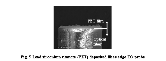
Recently,
Iwanami et al. has made a breakthrough regarding this aspect of optical fiber
based EO sensing devices [16-18].
They have succeeded in direct depositions of EO crystal (lead zirconium
titanate: PZT) films on an optical fiber facet. A scanning electron micrograph of a
device thus fabricated is shown in Fig. 5.
One should note that the area of the EO crystal is almost the same as
that of an optical fiber facet or even smaller. This feature is considerably attractive
as follows. (a) The shape and size
of the EO crystal, which has been a limiting factor of the EO probe head size,
is no longer larger than the optical fiber facet diameter. Hence, the easy-to-insert-anywhere
feature of the fiber-edge scheme is highly enhanced. (b) One can reduce the thickness of the
crystal down to the nanometer range if desired. In combination with optical fibers of
finer core diameters, the minimum sensitive volume can be reduced down by one
order of magnitude or more. It may
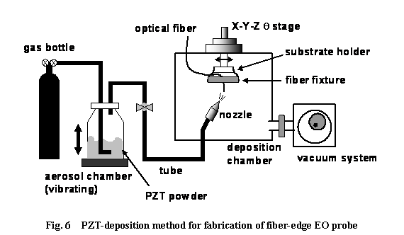
lead to creation of new EO measurement paradigm. Fig. 6 shows a schematic of the aerosol
deposition method, which was utilized for the EO sensing device
fabrication.
III.
LN disk resonator for EO sensing
One of the most effective methods
to improve the sensitivity of an EO probe is to enlarge the interaction length
between a light-wave and an electrical signal to be measured. Usages of optical cavities are
fairly effective for this purpose since the interaction length is effectively
enlarged by a cavity quality factor (Q factor) [9], provided that the
measurement bandwidth suppression given by the corresponding photon lifetime of
cavity can be managed somehow for practical measurements. Recently, as well known, high-Q optical
cavities are available, mainly on the basis of optical disk resonator scheme
and its whispering gallery mode (WGM).
Especially, It has been reported that a cavity having a Q factor of 108
or more can be made of an EO crystal [19][20].
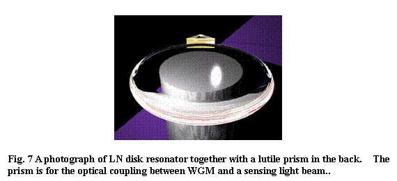
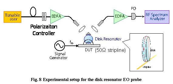
Sasagawa and Tsuchiya have
performed an experiment in which such a high-Q cavity is applied to the EO
sensing scheme [21-24]. The LiNb3
(LN) disk resonator which they made is shown in Fig. 7 and the relevant
experimental setup is indicated in Fig. 8.
The axis of disk rotation symmetry is parallel to the c-axis of LN
crystal. A sensing light beam is
coupled to the LN disk resonator trough a rutile prism, which is shown in the
upper part of Fig. 7. The radius of
the disk is 3.3 mm while its rim curvature radius is 3.3 mm. The LN disk resonator, an EO sensing
head in other words, was allocated on a micro stripline as shown in Fig. 8,
which is a device-under-test (DUT) in the measurement. Thus, some evanescent
waves of RF signals in the stripline were measured and the sensitivity was
investigated.
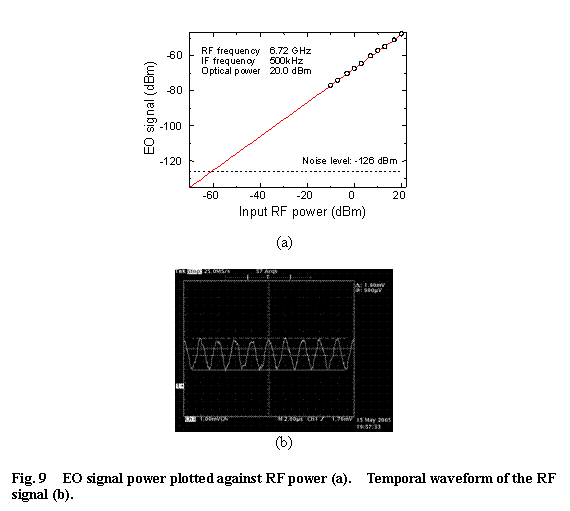
Figures 9 show (a) EO signal power
thus obtained at the RF spectrum analyzer in Fig. 8, which is plotted against the
RF power launched to DUT, and (b) a temporal waveform measured by a
oscilloscope for a photonically down-converted IF signal at 500 kHz. The frequency of the original RF signal
is 6.72 GHz and the impedance of the stripline is 50 W . Note that the estimated minimum
detectable RF power on the stripline is as low as -60 dBm, which corresponds to
the minimum detectable voltage of 0.13 mV/Hz1/2. Those values indicate the highest EO
sensitivity ever reported. Such a
high sensitivity allows one to observe the temporally sinusoidal waveform with
a digital oscilloscope as shown in Fig. 9 (b), which is rather difficult in the
EO sensing scheme conventionally.
IV.
Live Electro-optic Imaging (LEI)
One of the most eye-catching
inventions in this field is the realization of ultra-parallel RF signal measurement
scheme and its application to the real-time visualization of RF electrical
field distributions. This was done
by Sasagawa and Tsuchiya, and the technology is called as LEI [5-8]. The degree of parallelism is 10,000,
which is outstanding in comparison with the conventional single channel nature
in standard RF measurements. The
availability of 10,000 parallel RF measurements thus obtained has led to the
real-time visualization of RF field distributions, live imaging in other words.
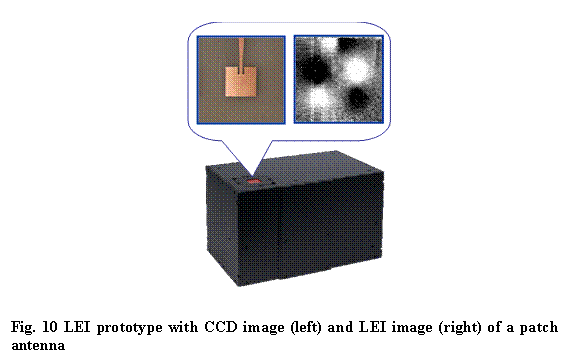
Shown in Fig. 10 is the latest
prototype of LEI camera provided by Sasagawa, Kanno, and Tsuchiya. The area of the prototype base is as
small as that of A4 letter paper size and therefore the prototype is portable. The insets of Fig. 10 are top view
pictures of a patch antenna taken simultaneously by the camera, which are by a
CCD image sensor (left) and a LEI view (right), respectively. One should note that intense electrical
fields are observed clearly on the four corners of the patch as conventionally
indicated by the electromagnetic theory.
The performance specifications of
the prototype are as follows. The
size of view area, which is located on the top surface, is 25 mm x 25 mm. Thus the device-on-the-top configuration
is brought about, which enables the face-down measurement scheme and eventually
easy-and-prompt handling of DUT for its RF field visualization. The observation bandwidth is as high as
10 GHz and the highest frame rate is 30 frames per second.
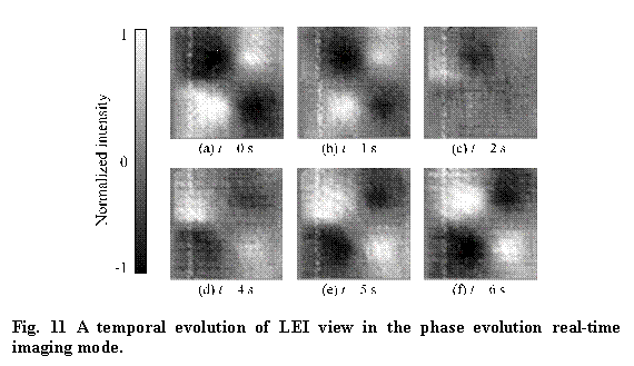
A series of images shown in Fig.
11 are taken from a LEI video stream and indicate a temporal evolution of the
LEI view for the patch antenna.
Here the LEI video stream was taken in the real-time mode with the phase
evolution imaging scheme. This was
made possible by intentional insertion of a slight discrepancy in frequencies
of the DUT signal and the LO signal, which is shown in Fig. 12 in more
details. Indeed, it is clearly seen
that the phase of DUT electrical field proceeds as the time goes.
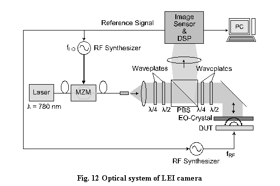
Figure
12 shows schematically the optical system of the LEI camera. One can see here that it includes rather
new elements of EO sensing scheme: the image sensor scheme listed in Fig. 1,
the EO heterodyne scheme listed in Fig. 3, and an EO plate of the fourth generation
shown in Fig. 4.
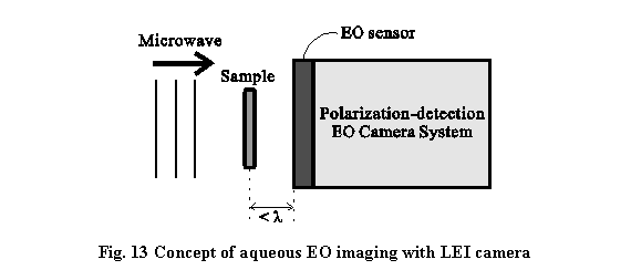
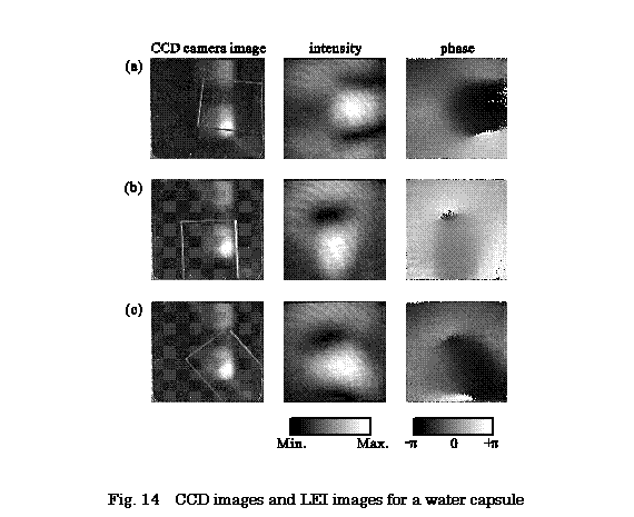
Kanno, Sasagawa, and Tsuchiya have
shown an interesting demonstration of LEI camera: its application to aqueous EO
imaging [25]. The imaging
configuration is shown in Fig. 13, where an aqueous sample is placed in front
of the sensing area of a LEI camera.
This configuration enables one to perform instantaneous characterization
of aqueous specimens. Examples are
shown in Figs. 14, in which high resolution images of transmitted microwave
intensity and phase distributions for a water capsule sample was successfully
obtained. Note that those were
obtained in less than one second.
Dramatic changes in EO intensity components at the edges of the sample
were visible, which is possibly due to diffraction of the incident
microwave. The phase components
clearly show the shape of the sample on the basis of absorption and phase
delay. Higher contrast in images
was obtained by the combination of the EO intensity and phase components:
phasor imaging.
[1]
M. Tsuchiya, “Methods for electromagnetic field measurements
with advantageous optical features employed”, the Review of Laser Engineering,
Vol. 33, No. 6 June 2005, pp. 365-372 (in Japanese).
[2]
S. Wakana, E. Yamazaki, M. Iwanami,
[3]
J. A. Valdmanis, G .Mourou, and C. W. Gabel,
“Picosecond electro-optic sampling system”, Applied Physics Letters, Vol. 41, No. 3,
pp. 211-212 (1982).
[4]
S. Wakana, T. Ohara, M. Abe, E. Yamazaki, M.
Kishi, and M. Tsuchiya "Novel electromagnetic field probe using
electro/magneto-optical crystal mounted on an optical-fiber facet for microwave
circuit diagnosis" Technical Digest of IEEE MTT-S International Microwave
Symposium 2000 (IMS2000), Boston, TH3C-3, pp. 1615-1618 (2000).
[5]
K. Sasagawa, and M. Tsuchiya: “Real-time
monitoring system of RF near-field distribution images on the basis of
64-channel parallel electro- optic data acquisition”, IEICE Electron. Express,
vol. 2, no. 24, pp. 600-606, December 2005.
[6]
K. Sasagawa, T. Kawanishi, and M. Tsuchiya:
“10,000 parallel heterodyne system for instantaneous photonics- based
acquisition of near-fields images over microwave devices/circuits”,
Asia-Pacific Microwave Conf. 2006, FR2C-5, pp. 1587-1590, December 2006.
[7]
K. Sasagawa, A. Kanno, T. Kawanishi, and M.
Tsuchiya: “Live electro-optic imaging of microwave near-fields via
ultra-parallel photonic heterodyne”, Int. Microwave Symp. 2007, WE1F-05, pp.
401-404, June 2007.
[8]
K. Sasagawa, A. Kanno, T. Kawanishi, and M.
Tsuchiya, “Live electro-optic imaging system based on ultra-parallel photonic
heterodyne for microwave near-fields,” IEEE Trans. Microw. Theory Tech., vol.
55, no. 12, pp. 2782-2791, December 2007.
[9]
S. Wakana, T. Ohara, M. Abe,
[10]
T. Ohara, M. Abe, S. Wakana, M. Kishi and M.
Tsuchiya, "RF Intensity mapping based on electro-optic spectrum
analysis", Technical Digest of Japan-Korea Joint Workshop on Microwave
Photonics, Osaka, W2-8, pp. 66-70 (2000).
[11]
T. Ohara, M. Abe, S. Wakana, M. Kishi, M.
Tsuchiya, and S. Kawasaki, "Two-dimensional field mapping of microstrip
lines with a band pass filter or a photonic bandgap structure by fiber-optic EO
spectrum analysis system", Technical Digest of Microwave Photonics 2000
(MWP 2000), Oxford, WE2.17, pp. 210-213 (2000).
[12]
[13]
E. Yamazaki, S. Wakana, M. Kishi and M. Tsuchiya
(Invited), “High
Frequency Magneto-Optic Probe Based on BiRIG Rotation Magnetization” , IEICE
Transactions on Electronics, Vol. E 86-C, No. 7, pp.1338-1344 (July, 2003).
[14]
S.
Wakana, E. Yamazaki, S. Mitani, H. Park, M. Iwanami, S. Hoshino, M. Kishi and
M. Tsuchiya, “Performance
Evaluation of Fiber-Edge Magneto-Optic Probe” , IEEE Journal of Lightwave
Technology, Vol. 21, No. 12, pp. 3292-3299 (December, 2003)
[15]
M. Iwanami, E. Yamazaki, K. Nakano, T. Sudo, S.
Hoshino, S. Wakana, M. Kishi and M. Tsuchiya, “Magnetic Near Field Measurements over LSI Package Pins by
Fiber-Edge Magnetooptic Probe”, IEEE Journal of Lightwave Technology, Vol. 21,
No. 12, pp.3273-3281 (December, 2003)
[16]
M. Iwanami, M. Nakada, H. Tsuda, K. Ohashi, and
J. Akedo, "Ultra Small Electro-optic Field Probe Fabricated by Aerosol
Deposition", IEICE Electronics Express, Vol. 4, pp. 26-32 (2007)
[17]
.M. Iwanami, M. Nakada, H. Tsuda, K. Ohashi, and
J. Akedo, "Ultra Small Fiber-Optic Electric Field Probe Fabricated by
Aerosol Deposition", Proc. 2007 Asia-Pacific Microwave Photonics
Conference (AP-MWP 2007), pp. 165-168 (2007).
[18]
M. Iwanami, M. Nakada, H. Tsuda, K. Ohashi, and
J. Akedo, "Ultra Small Magneto-optic Field Probe Fabricated by Aerosol
Deposition", IEICE Electronics Express, Vol. 4, pp. 542-548 (2007).
[19]
D. A. Cohen, M. Hossein-Zadeh and A. F. J. Levi,
“Microphotonic modulator for microwave receiver”, Electron. Lett. Vol. 37, pp.
300-301 (2001).
[20]
V. S. Ilchenko, A. A. Savchenkov, A. B. Matsko,
and Lute Maleki, "Nonlinear Optics and Crystalline Whispering Gallery Mode
Cavities," Phys. Rev. Lett. 92, 043903 (2004).
[21]
K. Sasagawa, and M. Tsuchiya, “An Electrooptic
Sensor with Sub-millivolt Sensitivity Using a Nonlinear Optical Disk
Resonator,” Int. Topical Meeting Microwave Photonics (MWP2005), F3-5, pp.
355-358,
[22]
K. Sasagawa, and M. Tsuchiya, “Stabilization of
whispering gallery resonance for highly sensitive EO sensor,” Contemporary
Photonics Technol. (CPT2006),
[23]
K. Sasagawa, and M. Tsuchiya, “A LiNbO3
disk resonator with a SiO2 cladding layer and proximate electrodes,” 2006
Conference on Lasers and Electro-Optics (CLEO 2006),
[24]
K. Sasagawa, and M. Tsuchiya, “Coating of SiO2
on a LiNbO3 optical disk resonator,” Contemporary Photonics Tech.
2007 (CPT2007),
[25]
A. Kanno, K. Sasagawa, and M. Tsuchiya,
“Instantaneous microwave transmission imaging of aqueous samples,” 2007
International Topical Meetings on Microwave Photonics (MWP 2007), Victoria, BC
Canada, Oct. 3-5, 2007, Th-3.5.
D2. Semiconductor Lasers
(Light sources for optical communication)
Semiconductor
laser is a key device both in the core and the periphery networks carrying
explosively increasing Internet traffics.
The transmission capacity of the each channel of WDM system has been
raised up to meet the increased traffics.
This section pays attention to development of the light sources for the
up-to-date optical communication networks, categorizing 4 application fields
depending on transmission distances.
1.
The ultra-short haul (<1km) transmission
The systems
using the combination of the Fabry-Perot laser and the multimode fiber (MMF)
are developed, which are capable of 10Gb/s bit rate with 300m distance
(IEEE802.11aq)[1]. Since reduction
of the cost of light source assembly is the most important issue the
vertical-cavity surface-emitting laser (VCSEL) is a promising light
source[2]. Characteristics of
driving current vs. light output of VCSEL chip can be measured on wafer because
its cavity is vertical to the wafer surface, which pushes down the overall
cost. Transmission distance and bit
rate of VCSEL are typically less than 600m and 1Gb/s, respectively.
2.
The short to medium haul (1-25 km) transmission
Since the
cost issue is still important even for the medium haul system the distributed feedback
(DFB) laser is used under direct current modulation scheme. However the lasing frequency fluctuation
during dynamic modulation (chirping) is unavoidable, which is caused by
injection current change followed by carrier density and refractive index
change in active region. This
results in transmitted waveform distortion because the wavelength dispersion
exists even in a single mode fiber (SMF).
One of the solutions of this problem is to use DFB laser emitting
1.3-micrns wavelength, in which the wavelength dispersion of SMF is nearly
zero.
The light source free from temperature
control reduces substantially the cost of the system. Carrier overflow from the quantum well
consisting of the active layer degrades temperature characteristics. Aluminum based mixed crystal is used
instead of Phosphorus based one to achieve large electron barrier height of
quantum well to prevent the carrier overflow. The dynamic single mode operation at
temperature rage of –40 to 85 degrees Celsius is achieved by Al based laser and
applied 10Gb/s system.
3.
The medium to long haul (25-80km) transmission
The narrower
line-width of optical source is demanded as longer transmission length. To
address this request the external modulator is used with cw DFB laser. For the medium haul system the
semiconductor electro-absorption (EA) modulator is used as the external
modulator and monolithically integrated with DFB laser. EA modulator based on the Quantum
Confined Stark Effect (QCSE) has electric field dependent sharp absorption edge
and is capable of more than 10dB extinction ratio even with 200 microns device
length, which realizes small optical sources. Moreover, layer structure of EA
modulator is similar to that of the laser, which makes it easy to integrate
monolithically each other and to reduce the fabrication cost. On the other hand there still remains
instantaneous frequency chirp caused by a refractive index change upon applied
electric field, which limits transmission length. Recently EA modulator with special core
structure is developed and successfully applied to the system with the fiber
dispersion of 1600ps/nm (corresponding to 80km-SMF). The integrated light source with the
temperature control free laser is developed and realized the operation
temperature of 90 degrees Celsius[3].
4.
The long to ultra-long haul (>80km) transmission
The
limitation coming from the chirping characteristic is much more strict for this
transmission length with more than 10Gb/s rates. The Mach-Zehnder (MZ) modulator is used
instead of the EA modulator. A MZ
modulator consists of dielectric material LiNbO3 is generally used for the
practical systems because of its chirp-less characteristics. However, there remain some difficulties
such as large size, large driving voltage, and drifting of driving voltage
balance. To address these problems
the semiconductor MZ modulator is developed with a footprint size comparable to
that of a semiconductor laser and capable of 40Gb/s modulation[4].
As an
advanced structure the DQPSK modulator composes of two MZ modulators is
developed and applied to the 80Gb/s modulation experiment[5]. The semiconductor integrated light
sources including modulators, lasers and other photonic devices are promising
for the future advanced communication networks[6].
References
[1]
Y. Kurihara et al., “10Gbit/s FP-TOSA and PIN-ROSA for 10GBASE-LRM
application”, OFC06, Technical Digest, OThN4, 2006.
[2]
N. Nishiyama et al., ”1.3 and 1.55-mm InP-based VCSELs for digital and radio
signal transmission”, OFC07, Technical Digest, OMK4, 2007.
[3]
S. Makino et al., “Wide temperature (15C to 95C), 80-km SMF transmission of a
1.55-mm, 10-Gbit/s InGaAlAs electroabsorption modulator integrated DFB laser,”
OFC07, Technical Digest, OMS1, 2007.
[4]
K. Tsuzuki et al., “1.3-Vpp push-pull drive InP Mach-Zehnder modulator module
for 40 Gbit/s operation,” ECOC '05, Technical Digest, Th2.6.3, pp. 905-906,
2005.
[5]
N. Kikuchi et al, “80-Gbit/s InP DQPSK modulator with an n-p-i-n structure,”
ECOC2007, Technical Digest, 10.3.1, vol. 4, pp. 143-144, Sept., 2007.
[6]
T. Yasui et al., “Lossless 10-Gbit/s InP n-p-i-n Mach-Zehnder modulator
monolithically integrated with semiconductor optical amplifier,” OFC’08,
Technical Digest, OThC5, 2008.
D3. Tbps optical
modulators
Optical
modulators using electro-optic (EO) or electro-absorption (EA) effect play
important roles in high-speed optical communication systems. Recently, over
20Tbps optical fiber transmission was demonstrated by using integrated lithium
niobate (LN) optical modulators for ultra high-speed differential phase shift
keying (DQPSK) signal generation [1, 2]. Intensity modulation (IM) and on–off
keying (OOK) are commonly used in commercial systems. However, recently,
various types of modulation techniques, for example, differential
phase-shift-keying (DPSK) [3], DQPSK [4–7], amplitude- and phase-shift-keying
(APSK) [8, 9], frequency-shift-keying (FSK) [10–14], single-sideband (SSB)
modulation techniques [15]–[17], etc., were investigated to obtain enhanced
spectral efficiency or receiver sensitivity in optical transmission systems.
Orthogonal modulation techniques with OOK and FSK or OOK and DPSK are also
attractive for optical labeling in optical systems [12, 18, 19]. Integrated LN
modulators, such as dual-parallel Mach-Zehnder modulators (DPMZMs),
quad-parallel Mach-Zehnder modulators (QPMZMs), etc., can generate advanced
modulation format signals, such as high speed 16QAM (see figure 1), whose
constellations are complicated [20, 21]. Precise lightwave control was also
investigated to achieve pure optical clock signal generation and
high-performance digital modulation [22, 23].
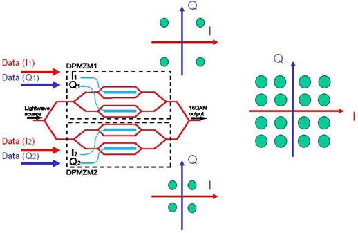
Fig.1 Optical 16-QAM
signal generation using a QPMZM [20]
[1]
A. H. Gnauck, G. Charlet, P. Tran, P. J. Winzer, C. Doerr, J. Centanni, E. Burrows,
T. Kawanishi, T. Sakamoto, K. Higuma, “25.6-Tb/s C+L-Band Transmission of
Polarization-Multiplexed RZ-DQPSK Signals,” presented at the OFC 2007,
Postdeadline Paper 19
[2]
H. Masuda, A. Sano, T. Kobayashi, E. Yoshida, Y. Miyamoto, Y. Hibino, K. Hagimoto,
T. Yamada, T. Furuta, H. Fukuyama, “220.4-Tb/s (204 × 111 Gb/s) Transmission
over 240 km Using Bandwidth-Maximized Hybrid Raman/EDFAs,” presented at the OFC
2007, Postdeadline Paper 20
[3]
A. H. Gnauck, G. Raybon, S. Chandrasekhar, J. Leuthold, C. Doerr, L. Stulz, and
E. Burrows, “25 × 40-Gb/s copolarized DPSK transmission over 12 × 100-km NZDF
with 50-GHz channel spacing,” Photonics Technol. Lett., vol. 15, pp. 467–469,
2003.
[4]
N. Yoshikane and I. Morita, “1.14 b/s/Hz spectrally efficient 50 × 85.4 Gb/s
transmission over 300 km using copolarized RZ-DQPSK signals,” J. Lightw.
Technol., vol. 23, no. 1, pp. 108–114, Jan. 2005.
[5]
A. H. Gnauck, P. J.Winzer, S. Chandrasekher, and C. Dorrer, “Spectrally
efficient (0.8 b/s/Hz) 1-Tb/s (25 × 42.7 Gb/s) RZ-DQPSK transmission over 28
100-km SSMF spans with 7 optical add/drops,” presented at the ECOC 2004,
Postdeadline Paper Th4.4.1.
[6]
R. A. Griffin, “Integrated DQPSK transmitters,” presented at the OFC 2005,
Paper OTuM1.
[7]
K. Ishida, K. Shimizu, T. Mizuochi, K. Motoshima, D. S. Ly-Gagnon, and K.
Kikuchi, “Transmission of 20 × 20 Gb/s RZ-DQPSK signals over 5090 km with 0.53
b/s/Hz spectral efficiency,” presented at the OFC 2004, Paper FM2.
[8]
N. Kikuchi,
[9]
T. Miyazaki, Y. Awaji, Y. Kamio, and F. Kubota, “Field demonstration of
160-Gb/s OTDM signals using eight 20-Gb/s 2-bit/symbol channels over 200 Km,”
presented at the OFC 2005, Paper OFF1.
[10]
W. Idler, A. Klekamp, R. Dischler, and B. Wedding, “Advantages of frequency
shift keying in 10-Gb/s systems,” presented at the 2004 IEEE/LEOS Workshop on
Advanced Modulation Formats, Paper FD3.
[11]
T. Kawanishi, T. Sakamoto, S. Shinada, M. Izutsu, K. Higuma, T. Fujita, and J.
Ichikawa, “LiNbO3 high-speed optical FSK modulator,” Electron. Lett., vol. 40,
pp. 691–692, 2004.
[12]
T. Kawanishi, T. Sakamoto, S. Shinada, M. Izutsu, K. Higuma, T. Fujita, and J.
Ichikawa, “High-speed optical FSK modulator for optical packet labeling,” J.
Lightw. Technol., vol. 23, no. 1, pp. 87–94, Jan. 2005.
[13]
T. Sakamoto, T. Kawanishi, T. Miyazaki, and M. Izutsu, “Novel modulation scheme
for optical continuous-phase frequency-shift keying,” presented at the OFC
2005, Paper OFG2.
[14]
T. Sakamoto, T. Kawanishi, and M. Izutsu, “Optical minimum-shiftkeying with
external modulation scheme,” Opt. Exp., vol. 13, pp. 7741– 7747, 2005.
[15]
M. Izutsu, S. Shikamura, and T. Sueta, “Integrated optical SSB
modulator/frequency shifter,” J. Quantum Electron., vol. 17, pp. 2225–2227,
1981.
[16]
T. Kawanishi and M. Izutsu, “Linear single-sideband modulation for high- SNR
wavelength conversion,” Photon. Technol. Lett., vol. 16, pp. 1534–1536, 2004.
[17]
D. D. Fonseca, P. Monteiro, A. V. T. Cartaxo, and M. Fujita, “Single sideband
demonstration using a four phase-modulators structure,” presented at the 2004
IEEE/LEOS Workshop on Advanced Modulation Formats, Paper FC2.
[18]
J. J. Vegas Olmos, I. Tafur Monroy, and A. M. J. Koon, “High bit-rate combined
FSK/IM modulated optical signal generation by using GCSR tunable laser
sources,” Opt. Exp., vol. 11, pp. 3136–3140, 2003.
[19]
K. Vlachos, J. Zhang, J. Cheyns, S. Nan Chi, E. Van Breusegem, I. Tafur Monroy,
J. G. L. Jennen, P. V. Holm-Nielsen, C. Peucheret, R. O’Dowd, P. Demeester, and
A. M. J. Koonen, “An optical IM/FSK coding technique for the implementation of
a label-controlled arrayed waveguide
packet
router,” J. Lightw. Technol., vol. 21, no. 11, pp. 2617–2628, Nov. 2003.
[20]
T. Sakamoto, A. Chiba and T. Kawanishi, “50-Gb/s 16 QAM by a
quad-parallel Mach-Zehnder modulator,” presented at the ECOC 2007,
Postdeadline Paper 2.8
[21]
Christopher R. Doerr, P. J. Winzer, L. Zhang, L. Buhl and N. J. Sauer,
“Monolithic 80-Gb/s Dual-Polarization On-Off-Keying Modulator in InP,”
presented at the OFC 2008, Postdeadline Paper 19
[22]
T. Kawanishi, T. Sakamoto, A. Chiba and M. Izutsu, “Study of precise optical
modulation using Mach-Zehnder interferometers for advanced modulation formats,”
presented at the ECOC 2007, 6.2.3,
[23]
T. Kawanishi, T. Sakamoto, A. Chiba, M. Izutsu1, P. J.Winzer, “Duobinary Signal
Generation Using High-Extinction Ratio Modulation,” presented at the OFC 2008,
OWL2
D4. Photonic Signal
Processing
The
final target of photonic signal processing is to realize all optical switching
and all optical logical processing, and very wide range of topics are
included. Recently, more sophisticated
signal processing is enabled due to the appearance of high power optical
sources and high-nonlinearity media.
The kinds of nonlinearity utilized are increasing and SHG (sum frequency
generation), DHG (difference frequency generation) and two photon absorption
are also utilized in addition to well-known XPM (cross phase modulation), FWM
(four wave mixing), Raman scattering and Brillouin scattering.
As for
optical fiber signal processing, concerns on optical pulse compression with CPF
(comb-like profiled fiber) and supercontinuum light generation with very
wideband, stable and excellent frequency characteristics are increasing. On wavelength conversion, many new
schemes with superior performance are proposed, using HNLF (high nonlinearity
fiber) and SOA (semiconductor optical amplifier) that both of them are used in
variation of configuration of MZI (Mach-Zehnder interferometer) and ring
interferometer.
Optical
functional devices are being advanced rapidly. For example, optical label recognition
of OCDMA (optical code division multiplexing) signal using SSFBG
(super-structured fiber Bragg grating) and optical logic device (bistable
device, optical memory, optical switch, optical NOR gate, etc.) are included. The papers on all optical regeneration
(2R and 3R) using these functional devices are often found.
K.
Igarashi, H. Tobioka, M. Takahashi, J. Hiroishi, T. Yagi, M. Sakano and S.
Namiki [2005], “Widely tunable sub-picosecond compression of 40 GHz
externally-modulated pulse train using 1.4 km long comb-like profiled fiber”,
OFC/NFOEC 2005, Optical Fiber Communication Conference, JWA6
M.
Naruse, T. Miyazaki, and F. Kubota, H. Yoshida and H. Ishikawa[2005],
“Ultrafast all-optical NOR gate based on intersubband and interband modulation
operating at communication wavelengths”, OFC/NFOEC 2005, Optical Fiber
Communication Conference, OFE3
J.
Suzuki, T. Tanemura, K. Tara, Y. Ozeki, and K.Kikuchi[2005], “All-Optical
Regenerator Using Wavelength Shift Induced by Cross-Phase Modulation in
Highly-Nonlinear Fibers”,OFC/NFOEC 2005, Optical Fiber Communication
Conference, OME64
H.
Furukawa, N. Wada and T. Miyazaki [2005], “Demonstration of 160 Gbit/s Optical
Packet Switching and Buffering Based on All-optical Code Label Processing”,
LEOS 2005, The 18th Annual Meeting of the IEEE Lasers and Electro-Optics
Society, pp.89-90
H.
Nishioka, K. Hayasaka, H. Tomita, K. Ueda[2005], “Frequency-domain phase
conjugator by a two-photon gated Bragg grating for nJ laser pulses”, LEOS 2005,
The 18th Annual Meeting of the IEEE Lasers and Electro-Optics Society,
pp.697-698
M.
Matsuura,
M.
Hattori, K. Nishimura, R. Inohara and M. Usami[2006], “New operation scheme of
SOA-MZI all-optical wavelength converter cancelling cross gain modulation”,
OFC/NFOEC 2006, Optical Fiber Communication Conference, OWS5
J.
Kurumida, H. Uenohara, and K. Kobayashi[2006], “All-optical Label Recognition
with SOA-MZI Multistage Switching Scheme”, OFC/NFOEC 2006, Optical Fiber
Communication Conference, JThB51
T.
Hamanaka, X. Wang, N. Wada and K. Kitayama[2006], “511-chip SSFBG and DFG-based
optical thresholder enabled compound data rate (10Gbps-622Mbps) OCDMA
experiment for multiple service provisioning platform”, OFC/NFOEC 2006, Optical
Fiber Communication Conference, OThT4
K.
Takiguchi, H. Takahashi, and O. Moriwaki and M. Okuno[2007], “Integrated
photonic decoder with complementary code processing and balanced detection for
two-dimensional OCDMA”, OFC/NFOEC 2007, Optical Fiber Communication Conference,
OWV5
H.
Furukawa, A. Nirmalathas, N. Wada, S. Shinada, H. Tsuboya, and T.
Miyazaki[2007],
“All
Optical Tunable Wavelength Conversion at > 160 Gb/s” , OFC/NFOEC 2007,
Optical Fiber Communication Conference, OTuI1
K.
Iwashita and K. Nakajima[2007], “Digitally Tunable Optical Frequency Converter
based on Optical SSB Modulators and Mach-Zehnder”, OFC/NFOEC 2007, Optical
Fiber Communication Conference, JWA56
H.
Tamai, M. Sarashina, K. Sasaki, and M. Kashima[2007], “First Demonstration of
Clockless Serial Optical Code Label Switching with SSFBGs Label Recognizer”,
OFC/NFOEC 2006, Optical Fiber Communication Conference, JThA72
K.
Takano, N. Hanzawa,
T.
Sakamoto, T. Kawanishi and M. Izutsu[2007], “Optimization of Electro-Optic Comb
Generation Using Conventional Mach-Zehnder Modulator”, MWP 2007, IEEE
International Topical Meeting on Microwave Photonics, pp.50-53
M.
Takenaka, K. Takeda, Y. Kanema, M. Raburn, T. Miyahara, H. Uetsuka and Y.
Nakano[2007], “MMI bistable laser
diode optical flip-flops for all-optical packet switching networks”, LEOS 2007,
The 20th Annual Meeting of the IEEE Lasers and Electro-Optics Society,
pp.652-653
G.
Hirano and F. Koyama[2007], “Slowing Light in Bragg Reflector Waveguide with
Tilt Coupling Scheme”, LEOS 2007, The 20th Annual Meeting of the IEEE Lasers
and Electro-Optics Society, pp.86-87
D5. THz Technology
Terahertz
(THz) electromagnetic waves, which cover an unexplored portion of spectrum
between infrared and microwaves at frequencies from 100 GHz to 10 THz, have
been expected to offer innovations in sensing, imaging, spectroscopy, and
communications. In Japan, several organizations, which contribute to accelerate
the THz science and technology in both academic societies and industries, have
been established; Terahertz Technology Forum, Technical Group on Terahertz
Application Systems in the Institute of Electronics, Information and
Communication Engineers (IEICE), Terahertz Technology Professional Group in the
Japan Society of Applied Physics (JSAP), Technical Group on Terahertz
Electromagnetic-wave Industrial Applications in Japan Science and Technology
Agency (JST), Division of Terahertz Spectroscopy in Spectroscopical Society of
Japan, etc.
Generation of
high power THz signals is the most important for the continuing advance of THz
technology. Photonic generation of THz signals based on photomixing in
nonlinear optical (NLO) crystals and photodiodes has been studied in the
continuous-wave (CW) as well as pulsed operations. Using an organic NLO
crystal, DAST (4-dimethylamino-N-methyl-4
stilbazolium tosylate), Suizu et al. succeeded in the generation of high
power THz waves up to mid-IR range. Ito et al. reported CW generation of 10
microwatts power at 1 THz using an antenna-integrated uni-traveling-carrier
photodiode (UTC-PD), which is the highest ever obtained with photodiodes.
Purely electronic devices have been examined with a resonant tunneling diode
(RTD) by Asada et al., and a Bloch oscillation by Hirakawa et al. A novel THz
emitter based on plasma-waves has been developed by Otsuji et al. A terahertz
quantum cascade laser (QCL) technology led by Hosako et al. is an alternative
promising approach, though a low-temperature operation is required. As for
THz-signal detection technologies, Komiyama et al. developed a highly-sensitive
THz detector, or a single photon counter based on quantum dots.
In recent
years, there have been increasing research and development on real-world
applications of the THz technology. They include measurement and sensing
systems, such as real-time THz spectrometer (Guo et al.), real-time 2D imaging
(Hattori et al.), detection of crystalline defects (Nishizawa et al.),
detection of illicit drugs in mail (Dobroiu et al.), detection of inflammable
liquids (Ikeda et al.), gas sensing (Song et al.), detection of protein
(Yoshida et al.), diagnostics of cancer tissues (Nakajima et al.), THz
spectroscopy in water and biological solution (Nagai et al.), compact sensor
chips for THz spectrometer (Kitagawa et al.), LSI testing (Yamashita et al),
measurement of paint film thickness (Yasuda et al.), etc.
There is an
urgent demand for higher data rate in wireless access systems in order to keep
up with the remarkable speed-up of fiber-optic networks. 10-Gbit/s data rate is
now required for the wireless transmission of 10-Gigabit Ethernet (10GbE)
signals, and multiplexed transmission of uncompressed high-definition
television (HDTV) signals. NTT has demonstrated the highest data rate of 10
Gbit/s using 120-GHz and 240-GHz carrier frequencies. Use of higher frequencies
of over 300 GHz is one of the trends from now on as the IEEE 802.15 Terahertz
Interest Group was launched in late 2007.
References
Asada,
M.,
Dobroiu,
A., Y. Sasaki, T. Shibuya, C. Otani, and K. Kawase [2007], “THz-wave
spectroscopy applied to the detection of illicit drugs in mail”, Proc. IEEE,
vol. 95, no. 8, pp. 1566-1575
Guo,
R., H. Minamide, T. Ikari, Y. Ishikawa, and H. Ito [2006], “Terahertz-wave
spectrometer based on a coherent terahertz-wave parametric generator”, Opt.
Hashiba,
H., and V. Antonov,L. Kulik,A. Tzalenchuk, P. Kleinschmid, S. Giblin, and S.
Komiyama [2006], “Isolated quantum dot in application to terahertz photon
counting”, Phys. Rev. B, vol. 73, 081310
Hattori,
T., K. Egawa,
Hattori,
T. and M. Sakamoto [2007], “Deformation corrected real-time terahertz imaging,”
Appl. Phys. Lett., vol. 90, no. 26, 261106
Hirata,
A., T. Kosugi, H. Takahashi, R. Yamaguchi, F. Nakajima, T. Furuta, H. Ito, H.
Sugahara, Y. Sato, and T. Nagatsuma [2006], “120-GHz-band millimeter-wave
photonic wireless link for 10-Gb/s data transmission”, IEEE Trans. Microwave
Theory Tech., vol. 54, no. 5, pp.1937-1944
Hosako,
I., N. Sekine, M. Patrashin, S. Saito, K. Fukunaga, Y. Kasai, P. Baron, T.
Seta, J. Mendrok,
Ikeda,
T., A. Matsushita, M. Tatsuno, Y. Minami, M. Yamaguchi, K. Yamamoto, M. Tani,
and M. Hangyo [2005],
“Investigation of inflammable liquids by terahertz spectroscopy”, Appl. Phys.
Lett., vol. 87, no. 3, 034105
Ito,
H., F. Nakajima, T. Furuta, T. Ishibashi [2005], “Continuous THz-wave
generation using antenna-integrated uni-travelling-carrier photodiodes”,
Semicond. Sci. Technol., vol. 20, no. 7 pp. S191-S198
Kitagawa,
J., T. Ohkubo, M. Onuma, and Y. Kadoya [2006], “THz spectroscopic
characterization of biomolecule/water systems by compact sensor chips”, Appl.
Phys. Lett., vol. 89, no. 4, 041114
Miyamaru,
F., M. Takeda, T. Suzuki, and C. Otani [2007], “Highly sensitive surface
plasmon terahertz imaging with planar plasmonic crystals”, Optics Express, vol.
15, no. 22 pp. 14804-14809
Nagai,
M., H. Yada, T. Arikawa, and K. Tanaka [2006], “Terahertz time-domain
attenuated total reflection spectroscopy in water and biological solution”, International
Journal of Infrared and Millimeter Waves, vol. 27, no. 4, pp. 505-515
Nagatsuma,
T. [2006], “Exploring sub-terahertz waves for future wireless communications”,
International Conference on Infrared and Millimeter-waves/Terahertz Electronics
(IRMMW-THz2006), PL-4, p. 4
Nagatsuma,
T., H. Ito, and T. Ishibashi [2007], “Photonic THz sources using
uni-traveling-carrier photodiode technologies”, Tech. Dig. IEEE LEOS Annual
Meeting, ThN3,
Nagatsuma,
T., A. Hirata, N. Kukutsu, and Y. Kado [2007], “Multiplexed transmission of
uncompressed HDTV signals using 120-GHz-band millimeter-wave wireless link”,
IEEE Intern. Meeting on Microwave Photonics, MWP 2007, pp. 237-240
Nagatsuma,
T. and Y. Kado [2007], “Microwave and millimeter-wave photonic devices for
communications and measurement applications”, Asia Optical Fiber Communication
and Optoelectronics Conference, AOE 2007, pp. 63-65
Nakajima,
S., H. Hoshina, M. Yamashita, C. Otani, and N. Miyoshi [2007], “Terahertz
imaging diagnostics of the cancer tissues with Chemometrics technique” Appl.
Phys. Lett., vol. 90, no. 4, 041102
Nishizawa,
J. T. Sasaki, K. Suto, T. Yamada, T. Tanabe, T. Tanno, T. Sawai, Y. Miura
[2005], “THz imaging of nucleobases and cancerous tissue using a GaP THz-wave
generator”, Opt. Comm., vol. 244, no. 1-6, pp. 469-474
Nishizawa,
J., K. Suto, T. Sasaki, T. Tanabe, T. Tanno, Y. Oyama, F. Sato [2006], “GaP
Raman terahertz high accuracy spectrometer and its application to detect organic
and inorganic crystalline defects”, Proceedings of the Japan Academy, Ser. B,
vol. 82, no. 9, pp. 353-358
Otsuji,
T., M. Hanabe, T. Nishimura [2006], “A grating-bicoupled plasma-wave photomixer
with resonant-cavity enhanced structure”, Optics Express, vol. 14, no.11, pp.
4815-4825
Song,
Ho-Jin, N. Shimizu, T. Furuta, K. Suizu, H. Ito, and T. Nagatsuma [2007],
“Broadband frequency tunable photonic sub-terahertz wave generation for
spectroscopic applications” Tech. Dig. IEEE LEOS Annual Meeting, ThF2, pp.
733-734
Suizu,
K., K. Miyamoto, T. Yamashita, and H. Ito [2007], “High-power terahertz-wave
generation using DAST crystal and detection using mid-infrared powermeter”,
Opt. Lett., vol.32, no.19, pp. 2885-2887
Syouji,
A., S. Saito, K. Sakai, M. Nagai, K. Tanaka, H. Ohtake, T. Bessho, T. Sugiura,
T. Hirosumi, and M. Yoshida [2007], “Evaluation of a terahertz wave spectrum
and construction of a terahertz wave-sensing system using a Yb-doped fiber
laser”, J. Opt. Soc. Am., vol. B 24, no. 8, pp. 2006-2012
Tonouchi,
M. [2007], “Cutting-edge terahertz technology”, Nature Photonics, vol. 1, no.2,
pp. 97-105
Ueno,
Y., R. Rungsawang, I. Tomita, and K. Ajito [2006], “Quantitative measurements
of amino acids by terahertz time-domain transmission spectroscopy,” Anal.
Chem., vol. 78, no. 15, pp. 5424-5428
Unuma,
T., N. Sekine, and K. Hirakawa [2006], “Dephasing of Bloch oscillating
electrons in GaAs-based superlattices due to interface roughness scattering”,
Appl. Phys. Lett. vol. 89, no. 16, 161913
Yamashita,
M., K. Kawase, C. Otani, T. Kiwa, M. Tonouchi [2005], “Imaging of large-scale
integrated circuits using laser terahertz emission microcopy”, Optics Express,
vol. 13, no. 1, pp. 115-120
Yasuda,
T., T. Iwata, T. Araki, and T. Yasui [2007], “Improvement of minimum paint film
thickness for THz paintmeters by multiple regression analysis”, Appl. Opt.,
vol. 46, no. 30, pp. 7518-7526
Yoshida,
H., Y. Ogawa, Y. Kawai, S. Hayashi, A. Hayashi, C. Otani, E. Kato, F. Miyamaru,
and K. Kawase [2007], “Terahertz sensing method for protein detection using a
thin metallic mesh”, Appl. Phys. Lett., vol. 91, no. 25, 253901
D6. Silicon Devices
Device
scaling of Silicon CMOS technology has enabled not only higher speed logic
circuits but also higher frequency analog/microwave circuits. As shown in Fig.
1, high frequency performance of typical NMOS transistors in 65 nm technology
node reaches their cutoff frequency fT and maximum oscillation
frequency fmax of over 200 GHz. The device scaling supported by wide
variety techniques, such as high-k dielectric gate insulator, low-k
interconnect insulator and thick Cu interconnect metal layer, enables also high
Q passive elements. In addition, Si CMOS technology, as well known, has
specific features of lower power consumption suitable to battery-driven mobile
devices, higher level integration of RF frontend and baseband circuits, and
lower fabrication cost in mass production, compared to the III-V compound
semiconductor (GaAs, InP) technology.
These high performance Si CMOS
analog/microwave circuits has started to prevail as RF frontend ICs in several
GHz frequency range applications, such as wireless local network (WLAN; IEEE
802.11a/b/g/n), 2G/3G cellar networks, worldwide interoperability for microwave
access (WiMAX; IEEE 802.16e), ultra-wideband impulse radio system (UWB-IR), and
electronic toll collection system (ETC). Many types of RF CMOS ICs [1-8] have
been developed such as low-noise amplifiers, voltage controlled oscillators
(VCO), up/down conversion mixers, power amplifiers, and multi-band multi-mode
transceiver ICs.
Recently millimeter wave
applications have much attention such as wireless personal area network (IEEE
802.15.3c) and wireless high-definition signal transmission system (Wireless
HD) in 60 GHz frequency range, and the vehicle radars including the short range
radars and long range radars for collision avoidance systems. The millimeter
wave is ideal for short-range high-capacity data transmission systems, as well
as for measuring with high resolution and accuracy the distance between two
points. Conventionally, the compound semiconductors have been used in the RF
front-end circuits of these systems in order to realize high gain, low noise
and high output power of high-frequency signals.
On the other hand, remarkable
progress in Si CMOS technology, besides SiGe:C BiCMOS [12-16], has been made in
regard to operational speeds and it is now possible to apply millimeter wave
circuits that were previously achieved through compound semiconductors.
Practical application, however, of Si CMOS technology in millimeter-wave
circuitry has been problematic due to the occurrence of significant signal loss
due to the conductive Si substrate and lack of an accurate device model up to
millimeter wave frequency range. Among millimeter-wave circuitry, power
amplifiers and VCO are key circuit blocks. As shown in Fig. 2, power amplifier
is one of the toughest targets due to the low-breakdown voltage of nm-scaled Si
CMOS transistors. In VCO its frequency tuning range is
significantly narrowed by the reduced ratio between the tuning varactor diode
to parasitic capacitance in the scaled devices. There were several reports
relating to technological challenges to overcome these problems [9-11].
Furthermore, by combining baseband circuit with RF front-end circuit on one
chip, millimeter-wave band transceiver chips - which had been expensive to
produce in the past - can now be made considerably smaller. As a result,
widespread applications of millimeter wave Si CMOS technology in both
automotive radar systems and wireless communications systems are anticipated in
the future.

Fig. 1 Trends of fT and fmax
Fig. 2 Output power of CMOS
power amplifiers
Reference:
Si
CMOS
[1]
T. Maeda, N. Matsuno, S. Hori, T. Yamase, T. Tokairin, K. Yanagisawa, H. Yano,
R. Walkington, K. Numata, N. Yoshida, Y. Takahashi, and H. Hida [2006], “A
Low-Power Dual-Band Triple-Mode WLAN CMOS Transceiver,” IEEE Journal of
Solid-State Circuits, vol. 41, pp. 2481–2490.
[2] T. Maeda, H. Yano, S. Hori, N. Matsuno,
T. Yamase, T. Tokairin, R. Walkington, N. Yoshida, K. Numata, K. Yanagisawa, Y.
Takahashi, M. Fujii, and H. Hida [2006], “Low-power-consumption
direct-conversion CMOS transceiver for multi-standard 5-GHz wireless LAN
systems with channel bandwidths of 5-20 MHz,” IEEE J. of Solid-State Circuits,
vol. 41, pp.375–383.
[3] K. Yanagisawa,
[4] R. Tachibana, S. Kousai, T. Kato, H.
Kobayashi, R. Ito, A. Maki, D. Miyashita, Y. Araki, T. Hashimoto, H. Hoshino,
T. Sekiguchi, M. Ashida, I. Seto, M. Hamada, R. Fujimoto, H. Yoshida, S. Otaka,
[2007], “A 0.13 m
CMOS 5GHz Fully Integrated 2x3 MIMO Transceiver IC with over 40dB Isolation”
IEEE Radio Frequency Integrated Circuits (RFIC) Symposium, pp. 661–664.
[5] T. Terada, R. Fujiwara, G. Ono, T.
Norimatsu, T. Nakagawa, K. Mizugaki, M. Miyazaki, K. Suzuki, K. Yano, A. Maeki,
Y. Ogata, S. Kobayashi, N. Koshizuka, K. Sakamura, [2007], “A CMOS UWB-IR
Receiver Analog Front End with Intermittent Operation,” IEEE Symposium on VLSI
Circuits, pp. 86 – 87.
[6] T. Norimatsu, R. Fujiwara, M. Kokubo, M.
Miyazaki, A. Maeki, Y. Ogata, S. Kobayashi, N. Koshizuka, K. Sakamura, [2007],
“A UWB-IR Transmitter With Digitally Controlled Pulse Generator,” IEEE J. of
Solid-State Circuits, vol. 42, pp. 1300 – 1309.
[7]
T. Terada, S. Yoshizumi, M. Muqsith, Y. Sanada, T. Kuroda, [2006], “A CMOS
ultra-wideband impulse radio transceiver for 1-Mb/s data communications and
±2.5-cm range finding,” IEEE Journal of Solid-State Circuits, vol. 41, pp. 891
– 898.
[8]
H. Sugawara, Y. Yoshihara, K. Okada, K. Masu, [2005],“Reconfigurable CMOS LNA
for software defined radio using variable inductor,” The European Conference on
Wireless Technology, pp. 547 - 550.
[9]
Y. Kawano, T. Suzuki, Y. Nakasha, T. Hirose, K. Joshin, [2007], “A 25-GHz,
40-mW Fully-Integrated Power Amplifier in Standard 90-nm Si-CMOS Technology,”
Korea-Japan Microwave Conference, pp. 17 – 20.
[10]
H. Shigematsu, T. Hirose, F. Brewer, and M. Rodwell, [2005], “Millimeter-wave
CMOS circuit design,” IEEE Trans. on Microwave Theory and Techniques, vol. 53,
pp. 472 – 477.
[11]
T. Mitomo, R. Fujimoto, N. Ono, R. Tachibana, H. Hoshino, Y. Yoshihara, Y.
Tsutsumi, I. Seto, [2007], “A 60-GHz CMOS Receiver with Frequency Synthesizer,”
IEEE Symposium on VLSI Circuits, pp. 172 – 173.
SiGe
BiCMOS
[12]
T. Oka, M. Hirata, Y. Ishimaru, H. Kawamura, and K. Sakuno, [2006], “SiGe HBT
Power Amplifier with Distortion-Controllable Bias Circuit and Its Application
to 802.11g Wireless LANs,” Proceedings of Asia-Pacific Microwave Conference,
pp. 133 - 136.
[13]
T. Nakamura, T. Masuda, N. Shiramizu, K. Washio, T. Kitamura, N. Hayashi,
[2006], “A Wide-tuning-range VCO with Small VCO-gain Fluctuation for Multi-band
W-CDMA RFIC,” Proceedings of the
32nd European Solid-State Circuits Conference, pp. 448 - 451.
[14]
S. Shinjo, K. Tsutsumi, K. Nakajima, H. Ueda, K. Mori, M. Hieda, J. Koide, M.
Inoue, N. Suematsu, [2006], “5.8GHz ETC SiGe-MMIC Transceiver having Improved
PA-VCO Isolation with Thin Silicon Substrate,” IEEE MTT-S International
Microwave Symposium Digest, pp. 2039 - 2042.
[15]
K. Tsutsumi, M. Kagano, and N. Suematsu, [2006], “A Double Tuned Ku-Band
SiGe-MMIC VCO with Variable Feed-Back Capacitor,” Proceedings of Asia-Pacific
Microwave Conference, pp. 1127-1130.
[16]
T. Nakamura, T. Masuda, K. Washio, H. Kondoh, [2007], “A Low-Phase-Noise
Low-Power 27-GHz SiGe-VCO using Merged-Transformer Matching Circuit Technique,”
IEEE Radio Frequency Integrated Circuits (RFIC) Symposium, pp. 413 - 416.
D7. A brief view on the
ultra wideband (UWB) status in
This
report summarizes current status of ultra wideband technologies in
1.
Standardizations
The
Association of Radio Industries and Businesses (ARIB),
Note: As
standardization activities on UWB radio systems, IEEE P802 standard committee
had engaged on 15.3a, for high data-rate UWB radio systems, and 15.4a, for low
data-rate systems. Two technologies competed in the 15.3a. One is a direct
sequence UWB (DS-UWB), which is a single-carrier UWB system using a spread
spectrum technology. Another one is a multiband OFDM (MB-OFDM), which is a
multi-carrier UWB system with 128 sub-carriers. The 15.3a was finally broken up
in January 2006 because none of the two technologies could win out. However,
the MB-OFDM was approved as ECMA-368 and 369 in December 2005. Later, it was
also published as ISO/IEC 26907 and 26908 in May 2007. The 15.4a, is an
impulse-based UWB radio system for low-rate wireless personal area networks. It
was published as an official standard of IEEE P802 in March 2007.
2)
Regulations
Japanese regulations on the UWB radio
systems were issued in August 2007. The permission PSD is -41.3 dBm/MHz in EIRP
over the frequency ranges of 3.4-4.8 GHz (low-band) and 7.25-10.25 GHz
(high-band). This is equal to the
Note: In the
3.
Research and development (R&D) activities
The R&D
activities in
References
[1]
http://www.arib.or.jp/english/html/overview/doc/5-STD-T91v1_0-E.pdf
[2]
A. Tanaka, H. Okada, H. Kodama, and H. Ishikawa, “A 1.1V 3.1-to-9.5GHz MB-OFDM
UWB Transceiver in 90nm CMOS,” IEEE ISSCC 2006, pp.398-407, Feb. 2006.
[3]
T. Norimatsu, R. Fujiwara, M. Kokubo, M. Miyazaki,Y. Ookuma, M. Hayakawa, S.
Kobayashi, N. Koshizuka, and K. Sakamura, "A novel UWB impulse-radio
transmitter with all-digitally-controlled pulse generator," Proceedings of
ESSCIRC 2005, pp.267-270, Sept. 2005.
[4]
S. Iida, K. Tanaka, H. Suzuki, N. Yoshikawa, N. Shoji, B. Griffiths, D. Mellor,
F. Hayden, I. Butler, J. Chatwin, "A 3.1 to 5 GHz CMOS DSSS UWB
transceiver for WPANs," ISSCC 2005, vol.1, pp.214-594, Feb. 2005.
[5]
T. Teshirogi, M. Ejima, M. Uchino, S. Saito, T. Kawamura, Y. Arayashiki, Y.
Sakamoto, T. Yoshida, Y. Watanabe, and A. Ishida, "UWB automotive radar to
mitigate impact on radio services using restricted band," Proceedings of
APMC 2005, vol. 1, Dec. 2005.
[6]
K. Takizawa, H.-B. Li, and R. Kohno, ” Wireless Vital Sign Monitoring using
Ultra Wideband-Based Personal Area Networks,” IEEE EMBS 2007, pp. 1798-1801,
Aug. 2007.
[7]
J. Wang and D. Su, "Design of an Ultra Wideband System for In-Body
Wireless Communications," The 2006 4th
D8. Body Area Network Devices
Wireless body area network, BAN or WBAN, consists of a
set of small intercommunicating wireless device having compact sensors, either
wearable or implanted into the human body, which can monitor vital information,
body movement, etc. These devices transmit data from the body to a base
station, from where the data can be forwarded to a hospital, clinic, home,
etc., in real time. Currently BAN systems are actively being discussed at
IEEE802.15.6 BAN standardization group [1]. Besides this standardization
activity, research and development on BAN are widely done for realizing
medical, health-care and entertainment applications having the frequency range
of 400 MHz (medical implanted communication system, MICS band) to 10.4 GHz (UWB
band) [2]. Radio propagation analysis and modeling around a body is
continuously investigated by using FDTD method or real propagation measurements
[4, 5]. One of the research topics needed to be addressed is that the BAN devices and its sensors used in BAN have to be low on complexity,
small in form factor, light in weight, power efficient, easy to use and
reconfigurable - especially for realizing a small and high-efficient antenna in
Figure 1 [6]. Considerable effort would be required to make BAN transmission
secure and accurate. It would have to be made sure that the patient’s data is
only derived from each patient’s dedicated BAN system and is not mixed up with
other patient’s data. Furthermore, the data generated from BAN should have
secure and limited access. To realize this, an easily inconvertible and
undecipherable device-chip structure is also investigated [3].

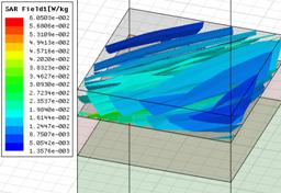
![テキスト ボックス: Figure 1 The implant’s antenna layout and its SAR distribution for designed implanted antenna at frequency of 403 MHz (Ref. [6]).](D08.files/image041.gif)
References
[1]
B. Zhen, H. Li, R. Kohno, "IEEE Body
Area Networks for Medical Applications," the 4th International Symposium
on Wireless Personal Communication Systems (ISWCS), 16 Oct. (2007)
[2] K. Takizawa, H. Li, K. Hamaguchi, R.
Kohno, "Wireless patient monitoring using IEEE802.15.4a WPAN,"
International Conference on Ultrawideband (ICUWB), 24, Sep. (2007)
[3] M. Kuroda, C. Li, R. Kohno, “A Study of
Energy-Efficient Authentication for Biosensor Nodes in Body Area Networks,” the
2nd International Symposium on Medical Information and Communication Technology
(ISMICT), 11-13 Dec. (2007)
[4] J. Wang, Y. Nishikawa,
"Characterization and Performance of High-Frequency Pulse Transmission for
Human Body Area Communications," IEICE Transactions on
Communications, Vol.E90-B, No.6, pp. 1344-1350, Jun. (2007)
[5] H. Yamamoto, T. Kobayashi,
"Measurements and Characterization of Ultra Wideband Propagation Channels
between a Base Station and On-Body Antennas", the 2nd International
Symposium on Medical Information and Communication Technology (ISMICT), 11-13
Dec. (2007)
[6] K. Y. Yazdandoost, R. Kohno, “An Antenna
for Medical Implant Communications System,” the 37th European Microwave
Conference (EuMC), pp.968-971, 8-12 Oct. (2007)
D9. Millimeter-Wave Antennas
The
research and development on millimeter-wave applications are getting hot again
in recent years, particularly in the field of millimeter-wave wireless
communication systems for high speed data transmission, such as millimeter-wave
wireless personal network (WPAN). Millimeter-wave antenna is an indispensable
device for such systems. Resent
research activities on millimeter-wave antennas in
High gain and
efficiency antenna array using waveguide-fed slot antenna structures. Compact and high gain/efficiency array
antennas have been developed for millimeter-wave wireless communications and
radars for vehicles at the operating frequencies from quasi-millimeter-wave to
60 GHz and 76-77 GHz bands.
Wideband and
relatively high-gain planar antenna have been developed for
quasi-millimeter-wave ultra-wideband system and for millimeter-wave WPAN. The developed antennas are of a
planar/multilayered structure antenna and a unique feeding/radiating structure
which realize a very compact, wide operating bandwidth and relatively high-gain
(~10 dBi) antenna. A configuration
and primary performance of the developed antennas for 60GHz millimeter-wave
WPAN are shown below.
NRD (Non-Radiative
Dielectric) waveguide antenna for millimeter-wave applications. NRD antenna can have a low transmission
loss and hence high radiation efficiency at 60 GHz 76-77 GHz bands. Works on integration of the NRD antenna
with the direct oscillator, mixer and other millimeter-wave circuits,
performing a simple millimeter-wave RF module, has been also carried out.
Beamforming/beam-steering
array antenna for millimeter-wave wireless communications and radars. The research and development are focused
on 60 GHz and 76-77 GHz bands, using switchable sector antenna or phased
antenna array to realize the beamforming/beam-steering performance required
from the systems.
New antenna
at millimeter-wave frequencies. New
material or new mechanism, particularly the use of metamatrial, has been
studied to realize some antenna performances such as wide beam steering.
Active
antenna Integrated with recent Si or SiGe CMOS devices. With the increasing operating frequency of
the recent CMOS devices, researches on the integration of such semiconductor
devices, including active circuits such as amplifier are paid attention for
developing future compact, efficient and easy-controlling antenna modules for
the millimeter-wave communication systems and radars.
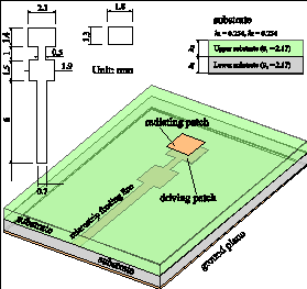
Fig. 1
Stacked patch antenna with two driving patches

(a) (b)
Fig. 2 Measured antenna performance:
(a) Return
loss and (b) Gain
Fig.
3 Measured radiation patterns in H-plane
of the developed antenna
(at
58 GHz, 60 GHz, 63 GHz, and 65 GHz, respectively)
References
[1]
Yasuhiro TSUNEMITSU, Goro YOSHIDA, Naohisa GOTO, Jiro HIROKAWA, and Makoto
ANDO, "The Ridged Cross-Junction Multiple-way Power Divider for Small
blockage and Symmetrical Slot Arrangement in the Center Feed Single-Layer
Slotted Waveguide Array,"IEICE Trans. Commun., Vol.E91-B, No.6, pp.-, Jun.
2008.
[2] Yasuhiro Tsunemitsu, Shigeru Matsumoto,
Yasuhiro Kazama, Jiro Hirokawa , and Makoto Ando, "Reduction of Aperture
Blockage in the Center-Feed Alternating-Phase Fed Single-Layer Slotted
Waveguide Array Antenna by E- to Hplane Cross-Junction Power
Dividers,"IEEE Transaction AP, communication. (to be published)
[3] Kaoru Sudo, Toru Oizumi, Jiro Hirokawa
and Makoto Ando "Reduction of Azimuthal Amplitude Ripple in the
Rotating-Mode Feed to a Radial Waveguide by Using a Crossed Dog-Bone
Slot," IEEE Trans. Antennas Propagat., vol.55, no.9, pp.2618-2622, Sept.
2007.
[4] Takafumi KAI, Yusuke KATOU, Jiro
HIROKAWA, Makoto ANDO, Hiroshi NAKANO, and Yasutake HIRACHI, "A Coaxial
Line to Post-Wall Waveguide Transition for a Cost-Effective Transformer between
a RF-Device and a Planar Slot-Array Antenna in 60-GHz Band," IEICE Trans.
Commun., Vol.E89-B, No.5, pp.1646-1653, May 2006.
[5]
[6] Y. Kimura, M. Takahashi, J. Hirokawa, M.
Ando, and M. Haneishi, "An Alternating-Phase Fed Single-Layer Slotted
Waveguide Array in 76GHz Band and Its Sidelobe Suppression," IEICE Trans.
Electron., Vol.E88-C, No.10, pp.1952-1960, Oct. 2005.
[7]
[8]Y.
Kimura, Y. Miura, T. Shirosaki, T. Taniguchi, T. Kazama, J. Hirokawa, M. Ando,
T. Shirouzu, "A Low-Cost and Very Compact Wireless Terminal Integrated on
the Back of a Waveguide Planar Array for 26 GHz Band Fixed Wireless Access
(FWA) Systems", IEEE Trans. Antennas and Propag., vol.53, no.8, pt.1,
pp.2456-2463, Aug. 2005.
[9]
Takuichi HIRANO, Jiro HIROKAWA, and Makoto ANDO, "A Design of a Leaky
Waveguide Crossed-Slot Linear Array with a Matching Element by the Method of
Moments with Numerical-Eigenmode Basis Functions," IEICE Trans. Commun.,
Vol.E88-B, No.3, pp.1219-1226, March 2005.
[10]
Keren Li, Naoki Kajitani, Kenneth K. F. Tong, and Toshiaki Matsui,
"Ultra-Wideband (UWB) Stacked Patch Antenna for Quasi-Millimeter-Wave
Application," Proceeding of
MINT-MIS2007/TSMMW2007/Millilab Workshop, vol.1, no. S2-1, pp.123-126,
[11]
Tomoaki Sato, Keren Li, Naoki Kajitani, Remi Roux, and Huan-Bang Li,
"Wideband Stacked Patch Antenna with Two Driving Patches for
Millimeter-wave Application (in Japanese)," 2007 IEICE Electronics Society
Symposium, B-1-2, pp. S-3, Sept. 2007.
[12]
Keren Li, and Tomoaki Sato, "Wideband Planar Antennas for Millimeter-Wave
Wireless Communications," 2008 IEEE AP-S International Symposium on
Antennas and Propagation and 2008 USNC/URSI National Radio Science Meeting in
San Diego, California, USA, on July 05-12, 2008.
[13]
T.Shimizu and T.Yoneyama, "NRD-Guide and Waveguide H-Plane Transition and
Its Application for Lens Antenna Feeding Structure," IEICE Trans.
Electron., vol.J89-C, no.5, pp.312-320, May. 2006.
[14]
T.Shimizu and T.Yoneyama, "Feeding Structures for 60GHz Dielectric Lens
Antenna with Low Sidelobes," IEICE Trans. Electron., Vol.J88-C, No.12,
pp.1096-1105, Dec. 2005.
[15]
T.Shimizu, T.Yoneyama, "A NRD Guide Fed Dielectric Lens Antenna with High
Gain and Low Sidelobe Characteristics," IEICE Trans. Electron., Vol.E88-C,
No. 7, pp.1385-1386, Jul. 2005.
[16]
Akifumi Hirata, Eddy Taillefer, Hiroyoshi Yamada, and Takashi Ohira,
"Handheld DOA Finder with Electronically Steerable Parasitic Array
Radiator Using the Reactance-Domain MUSIC Algorithm," IEEE Proceedings
Microwaves, Antennas & Propagation, 2007, 1, (4), pp.815-821, Aug. 2007.
[17]
Qing Han, Nobuyuki Tenno, Amane Miura, Masazumi Ueba and Takashi Ohira,
"Radial Fed SP8T Varactor-Mounted Waveguide Switch for Millimeter-Wave
Beam Steerable Antenna," 2007 IEEE AP-S International Symposium and
USNC/URSI National Radio Science Meeting, pp.4377-4380, Jun. 2007.
[18]
Qing Han, Nobuyuki Tenno, Amane Miura and Takashi Ohira, "Tapered Radial
Fed Circuit and Varactor-Mounted Waveguide Switch for Millimeter-Wave Switched
Sector-Beam Antenna," International Workshop on Antenna Technology 2007_,
pp.295-298, Mar. 2007.
[19]
Nobuyuki Tenno, Amane Miura, Takashi Itoh, Makoto Taromaru and Takashi Ohira,
"A Fundamental Study on a Switched-beam Sector Slot-array Antenna in 60GHz
Band," 2006 International Symposium on Antennas and Propagation, pp.1-5,
Nov. 2006.
[20]
Qing Han, Munehisa Yabuzaki, Makoto Taromaru, Takashi Ohira and Masami Akaike,
"Radial Fed Circuit For Millimeter-Wave Switched Sector-Beam Antenna,"
2006 IEEE AP-S International Symposium and USNC/URSI National Radio Science
Meeting , pp.3447-3450, July 2006.
[21]
S.-i. MATSUZAWA, K. SATO, A. SANADA, and H. KUBO, "Gain Improvement of a
Microstrip Composite Right/Left-Handed Leaky Wave Antenna Using Symmetrical
Unit Cells with Short Stubs,"
IEICE Trans B: Communications, E90-B(6): 1559 - 1561, June 1, 2007.
[22]
Shin-ichiro Matsuzawa, Kazuo Sato, Yoshinori Inoe, Tsuyoshi Nomura,
"Millimeter-Wave Steerable Composite Right/Left-Handed Leaky Wave Antenna
for Automotive Applications," IEICE Technical Report, vol. 106, no. 48,
MW2006-24, pp. 69-72, May 2006.
[23]
M. Sasaki, “Design of a Millimeter-Wave CMOS Radiation Oscillator With an
Above-Chip Patch Antenna,” IEEE
Trans. Circuits Syst. II, Vol. 53, No.10, pp.1128-1132, 2006.